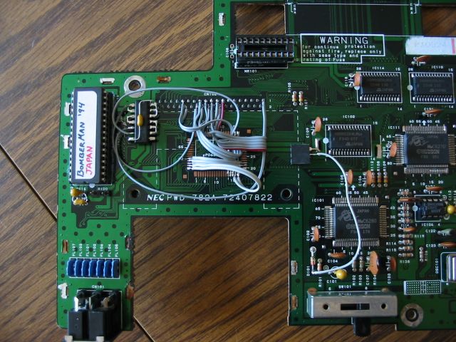
I was doing some rework on my TurboGrafx and decided to poke around at the unpopulated chip pads for IC107 and IC108 near the HuCard slot.
I've seen literature claiming these may have been intended for a built-in game. But after tracing back the pinout of both chips it looks more like IC107 was just supposed to contain a small instruction screen which is displayed when you start the console without a card (like the Master System). IC108 controls the mapping, and probably was just supposed to obfuscate the address line mapping of IC107 to make it more difficult to install stolen software.
But that's just a guess.
Anyway, with some work we can install our own built-in game up to 8 MEGA POWER in size. What we're going to do is adapt the original socket to hold a 27C801 compatible chip and add a small circuit to activate this ROM if and only if a HuCard isn't inserted. I'd rate this at moderate difficulty if you'd like to try, i.e. you should have some basic electronics knowledge and steady hands.
Let's do some soldering.
Here's the pinout for IC107 :
                 IC107
              _____ _____
         VCC | 1   v  32 | VCC
         OEn | 2      31 | R139 *
         GND | 3      30 | GND
         GND | 4      29 | GND
 ** IC108,18 | 5   2  28 | GND
 ** IC108,19 | 6   3  27 | IC108,17 **
 ** IC108,20 | 7   C  26 | IC108,16 **
 ** IC108,21 | 8   1  25 | GND
 ** IC108,22 | 9   0  24 | GND
          A2 | 10  0  23 | GND
          A1 | 11  0  22 | IC108,15 **
          A0 | 12  E  21 | D7
          D0 | 13     20 | D6
          D1 | 14     19 | D5
          D2 | 15     18 | D4
         GND | 16     17 | D3
             |___________|

  * R139 isn't populated, so this is NC'd.
    Looks like it was just supposed to be a pullup.

 ** IC108 isn't populated, so these are NC'd.
We need to modify it like this :
                                         IC107
                                      _____ _____
              *** A19 (HuCard Pin 3) | 1   v  32 | VCC
              *** A16 (HuCard Pin 4) | 2      31 | A18 (HuCard Pin 33)
              *** A15 (HuCard Pin 5) | 3      30 | A17 (HuCard Pin 32) ***
              *** A12 (HuCard Pin 6) | 4      29 | A14 (HuCard Pin 31) ***
  **** A7 (HuCard Pin 7) <- IC108,18 | 5      28 | A13 (HuCard Pin 30) ***
  **** A6 (HuCard Pin 8) <- IC108,19 | 6   2  27 | IC108,17 -> A8 (HuCard Pin 29)
  **** A5 (HuCard Pin 9) <- IC108,20 | 7   7  26 | IC108,16 -> A9 (HuCard Pin 28)
 **** A4 (HuCard Pin 10) <- IC108,21 | 8   C  25 | A11 (HuCard Pin 27) ***
 **** A3 (HuCard Pin 11) <- IC108,22 | 9   8  24 | OEn (HuCard Pin 26) ***
                                  A2 | 10  0  23 | A10 (HuCard Pin 25) ***
                                  A1 | 11  1  22 | IC108,15 -> GAME_CSn
                                  A0 | 12     21 | D7
                                  D0 | 13     20 | D6
                                  D1 | 14     19 | D5
                                  D2 | 15     18 | D4
                                 GND | 16     17 | D3
                                     |___________|

  *** Original trace must be cut.

 **** You can also just reconnect these address pins on IC108's pad.
      A7 == IC108,18 -> IC108,64
      A6 == IC108,19 -> IC108,63
      A5 == IC108,20 -> IC108,62
      A4 == IC108,21 -> IC108,61
      A3 == IC108,22 -> IC108,60
The circuit to enable the internal game (GAME_CSn) when a card isn't inserted can be two NAND gates using A20 (HuCard Pin 24) and CARDn (HuCard Pin 1).
GAME_CSn = !(!(A20 & A20) & CARDn)
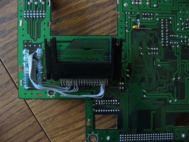
This can be implemented with a single 74LS00. Below are two photos of my board to give an idea of how much stuff you'll have to add.


Keep in mind some of the patch wires here are for different repairs or from when I was reverse engineering stuff. Basically, doing this won't make such a huge mess.